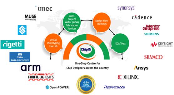 The Government of India is empowering universities across the country by providing access to industry-grade Electronic Design Automation (EDA) tools and Multi-Project Wafer (MPW) fabrication services, a significant step toward creating a large-scale semiconductor development ecosystem. During his visit to the Semiconductor Laboratory (SCL), Mohali, on 28th November 2025, Union Minister for Electronics & IT, Ashwini Vaishnaw, handed over 28 fabricated chips—including 600 bare dies and 600 packaged chips—designed by students from 17 academic institutions under the Chips to Start-up (C2S) Programme, showcasing India’s growing capabilities in chip design and fabrication. “This kind of large-scale semiconductor development ecosystem is unique to India,” he noted, highlighting the nation’s rapid emergence as a global leader in the semiconductor sector. The ChipIN Centre, established at C-DAC Bangalore, serves as a central hub providing advanced design workflows, compute infrastructure, IP cores, and mentorship, supporting academic institutions and start-ups by facilitating design verification, fab-compliance checks, and coordination with SCL for fabrication. Every three months, student-designed chips are aggregated onto a single MPW reticle, optimizing cost and time for fabrication. Over the past year, five MPW shuttle runs enabled 122 student design tapeouts from 46 institutions, with 56 chips successfully fabricated and delivered. More than 1 lakh students and 90 start-ups collectively utilized 175 lakh hours of EDA tools, making this one of the world’s largest centralized chip-design facilities. Vaishnaw emphasized that this initiative aligns with Prime Minister Narendra Modi’s vision of making India a self-reliant semiconductor powerhouse, reducing dependence on foreign technology, and promoting indigenous chip development. By providing hands-on experience to students and strengthening India’s semiconductor ecosystem, the programme positions the country as a global hub for chip design and fabrication.


Nurturing Creativity – Keekli Charitable Trust, Shimla